
Building an FM Radio on an FPGA
This post introduces a library for creating efficient FPGA-based digital filters written in the hardware description language Clash. I then use the library to implement an FM radio receiver on an FPGA. This post is also a continuation of my earlier blog posts on building a software fm radio receiver, and building some basic digital filters.
The source code for the radio can be found here.
Introduction
The design is a direct port of my software FM radio. While the signal processing is the same, an efficient implementation in digital logic is quite different to one in software. The digital filters that make up the majority of the logic are the main topic of this post.
In software, filters are usually implemented as nested loops. On an FPGA, we need structures like those described here, and more, in order to make efficient use of the limited resources available on the FPGA. In this post, I will extend those structures to further take advantage of patterns in the filter coefficients and the required data processing rates.
The result is a library of generic and reusable FIR filter structures inspired by, and providing a useful subset of the functionality provided by the Xilinx FIR compiler. In the end, we can fit an FM receiver (several, in fact) on our resource constrained Artix 7 FPGA.
Platform
I’ll be using the Arty 35T board to build the radio. The key metric for determining an FPGA’s DSP capabilities is the number of DSP slices it has. The FPGA on the Arty has 90 DSP slices. Each DSP slice is, roughly speaking, an adder, followed by a multiplier, followed by an adder. Each operation is optional and can be bypassed.
The Arty doesn’t have an RF frontend, so we need to stream samples over Ethernet to the FPGA from a device that does. For this purpose, I’m using an RTLSDR device. The RTLSDR is a cheap TV tuner that has an undocumented mode that streams raw samples from a frequency band of interest over USB and into software land. Once in memory, those samples are streamed back out over Ethernet for processing on the FPGA.
I’ve also written some simple software to stream the audio samples back from the FPGA, over Ethernet, and out my speakers. At a high level, the system looks like this:

Efficient filter design library
As mentioned above, the key FPGA metric for doing signal processing is the number of DSP slices available. A simplified diagram of a DSP slice is given in the figure below. All of the filters are designed around these blocks. If we want our filters to be efficient, we need to make sure they map nicely to this architecture.

The (simplified) DSP slice has four inputs. A and B are optionally summed (the A input can be muxed in instead of the adder output) and the output is fed into an optional pipeline stage. Next, the summed value is multiplied by C and then optionally accumulated with a cascade in signal from the DSP block below this one in the column.
Since the FPGA on the Arty board has 90 of these DSP slices, so we need to make sure our design fits within that. With that in mind, the next sections are about different filter structures that exploit properties of the filter coefficients and data rates to efficiently utilise DSP resources.
Multiplexing DSPs
In a previous post I focussed on filters that processed one sample per cycle. However, you usually don’t have to process a sample every cycle. For example, our Ethernet streaming system only gets us one complex sample to process every four cycles.
We can save resources in this case by time-multiplexing the DSP blocks. We hold previously received samples in a delay line. Every time a sample is received we spend the next few cycles multiplying and accumulating delay line samples and coefficients, before we can accept another new sample. By splitting and assigning banks of the filter coefficients to different DSP blocks we can arbitrarily trade throughput for DSP block usage.
For example, it would take 100 multipliers to build a transpose FIR filter with 100 coefficients that accepts one (real) sample per cycle. By multiplexing DSP blocks you could build this with only 50 multipliers if you only had to accept a sample every two cycles. Or, you could build this with a single multiplier if you only had to process one sample every 100 cycles.
These are referred to as semi-parallel filters in the source because a fully parallel filter would process all coefficients in one cycle. The implementation can be found here.
Filter coefficient symmetry
Digital filters are usually linear phase. Linear phase filters have symmetric coefficients, and you can exploit this symmetry to reduce the number of multipliers needed.
There are some details in my previous post but the idea is to use the pre-adder (that sums the A and B registers) in the DSP block to pre-sum the samples which would be multiplied by the same coefficient (at symmetric positions in the filter coefficient array), before doing the multiplication. This halves the number of multipliers needed for the same filter length.
Doing this is a little involved if you want it to also be a semi-parallel filter, since you need to read one half of your sample delay line in reverse, while making sure you have the sample needed to pass onto the next stage as needed. Details are in the code.
Polyphase decimation
Another trick is to reduce the computation needed when decimating by only computing the samples we actually need. Suppose we are decimating by a factor of 2, the most straightforward way to do this is to filter to remove aliases, then drop every second sample.
However, it is more efficient to not compute the dropped samples in the first place. This probably seems obvious. If you were implementing this in software, you would just adjust your loop to compute every second sample. However, it’s not so easy to do that directly with the hardware-centric structures discussed above.
The solution, in hardware, is the polyphase filter structure. You split your filter coefficients into multiple phases, then implement filtering for each phase at a lower rate. Since each sub-filter operates at a lower rate you can use the DSP multiplexing technique above to reduce the number of multipliers used in each filter.
Suppose you are decimating by a factor of 2. You split your filter into 2 sub-filters, one containing the odd coefficients, and the other containing the even coefficients. You now have two filters but each phase is now half the size and operates at half the rate. Overall, you halve your multiplier usage. Code is here.
Half band
In the special case of decimating by a factor of 2, splitting the filter response into two phases has another benefit. If we have a half band filter, which we will often have if we are decimating by a factor of 2, then one of our phases will be almost entirely zeros. In fact, there will only be a single non-zero coefficient in the second phase. The means the filter for the second phase is trivial, doesn’t use any multipliers, and we have another factor of 2 saving. Implementation is here.
Testing
It is very easy to make mistakes when building filters combining the optimisations above. There are so many corner cases that it is impossible to be confident in the filter’s designs without a comprehensive randomised testbench. One of the strengths of Clash is that every Clash design is also a valid Haskell program. This means that the entire Haskell testing ecosystem, including QuickCheck is available for testing Clash designs.
Everything is tested by comparing it to a golden reference model, which is assumed correct. The model is a direct form FIR filter (the simplest kind) and is just a few lines of code. The tests generate random filter coefficients and input data, run these through the reference model and DUT (design under test), and check that the outputs are identical. One of the filters is also formally verified using SymbiYosys, and I plan to verify the rest as well.
Performance
I synthesized the filters and verified that they map to DSP blocks and shift registers as I was expecting. Additionally, the greatest logic depth for any standalone filter is 3 (usually including a DSP block), so the filters will work well at high clock frequencies.
FM Radio Design
Now I’ll put the filters together to build a radio! The design is an FPGA port of the software FM radio described in a previous blog post. I recommend reading that if you want more details on the FM reception process, but the high level structure is shown in the figure below.

RF decimation
Decimation is needed because the RTLSDR device provides samples at a much higher rate than the bandwidth of the FM signal. Decimation is used to reduce the sample rate from 1.536MHz at the input to 192KHz for the next block (demodulation). RF decimation is efficiently achieved with three stages of semi-parallel polyphase symmetric half band filters (that’s a bit of a mouthful). Each stage decimates by a factor of 2, to give an overall decimation of 8.
Each decimation filter has an impulse response that is 128 samples long. As the filter is symmetric and half band, we can express that with 32 distinct non-zero real coefficients.
The first decimator in the chain uses the DSP multiplexing and polyphase decimation tricks to divide the coefficients into four banks of 8 coefficients. This reduces the number of complex multipliers from 32 to 4 (the number of banks) by only accepting a sample every 4 cycles, and outputting one every 8 (as we are decimating by 2). Since each complex by real multiplication uses two multipliers, the filter uses 8 DSPs for coefficient multiplication.
The second decimator only needs to accept a sample every 8 cycles, since the rate was halved by the first decimator in the chain. The resulting usage is 4 DSPs for coefficient multiplication. Lastly, with the rate halved again, the final decimator requires only 2 DSPs for coefficient multiplication.
Demodulation
Demodulation of an FM signal amounts to finding the phase of the complex samples and calculating the rate at which it changes. On an FPGA, we can’t simply call an arctangent function to get the phase of the current sample. We need to implement it ourselves, making sure that the resource usage and timing characteristics of the implementation are acceptable.
I use the elegant CORDIC algorithm to calculate the phase of the complex samples (implemented here in Clash). It does this without requiring a single multiplication!
Audio decimation
Audio decimation is almost exactly the same as RF decimation, except the samples are real instead of complex numbers. Real numbers are used because the CORDIC algorithm in the previous step outputs real numbers representing the phase difference of successive input samples.
Audio decimation takes the sample rate from 192KHz at the output of the demodulator, to 48KHz, the sample rate accepted by my sound card. There are two stages, each decimating by a factor of two. Both stages are organised as a single 32 coefficient bank, requiring only a single DSP for multiplication.
Final audio filter
The final audio filter strips out the pilot tone (see my previous post for details). It exploits the symmetry of the coefficients for a factor of 2 saving in multipliers compared to the naive implementation. Unfortunately, the polyphase optimisation doesn’t apply here because we’re not decreasing the sample rate, and the half band optimisation doesn’t apply since our filter doesn’t cut off in the middle of the band.
The filter has 64 coefficients. Again, we use a single bank since the sample rate is so low after all the decimation. The filter therefore uses a single multiplier.
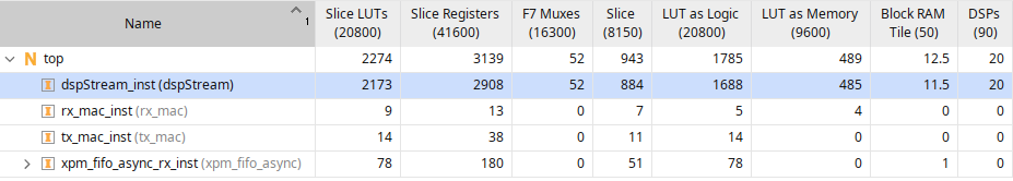
Synthesis
The utilization report is shown in the screenshot below. As you can see, the design uses 20 DSP blocks. If you add up all the DSP usages for coefficient multiplication above, you get 17 DSPs. In addition, the semi-parallel filters each require additional DSPs for an accumulate and dump operation. Three of these are accumulating complex values, and three are accumulating real numbers, giving 9 DSPs for accumulation operations. So, by my count, 26 DSPs should be in use. I guess Vivado was able to optimise some out, or replaced them with regular adders.
I should also add that the design functions as intended. When the FPGA is programmed and the system is setup as described in the platform section, the audio of my chosen FM station plays through my speakers with high quality.
Conclusion
I have introduced a library written in Clash for building resource efficient FPGA based digital filters, and used it to create a simple FM radio. In the future, I plan to build more complex designs capable of transmitting and receiving digital data. These will be based on software transmitters and receivers I’ve implemented here.