
Inspecting Ethernet Waveforms using FPGA Transceivers
In this post, I walk through the design of a sampling oscilloscope built using only the transceiver eye scan functionality of a Xilinx FPGA. A sampling oscilloscope lets you see the full analog waveform coming into the transceiver. I think it is neat that, with a few tricks, you can do this with only a Xilinx GTY, which, functionally, only provides a single 1 or 0 per bit period. It’s also nice to see what these high speed serial waveforms are actually doing in the time domain at the receiver.
I then use my new gigasample/s scope to examine the effect of data rates, cable lengths, and the GTY equalizer on the received waveform.
Background
A sampling oscilloscope (well explained here) works by sampling a periodic signal over many passes which sweep across the period. Each sample is performed at a slightly different offset in the periodic waveform. This allows a sampling oscilloscope to operate at a lower frequency (1 / the period), while still allowing us to see the details of what the waveform is doing within the period.
While the sampler operates at a lower frequency, it still needs to provide an accurate sample of the waveform at the precise instant it is triggered. It would be no good if it only provided, say, an average over some large fraction of the period. We’re going to build this functionality using using a Xilinx transceiver.
Xilinx transceivers can receive data correctly even if the channel suffers from considerable impairments. However, in the presence of too much attenuation or noise, the mechanisms built into the transceivers to overcome these impairments can be overwhelmed. This can happen, for example, with dodgy cables or poor PCB design. To debug these sorts of issues, Xilinx provides eyescan functionality within the transceiver, and this is what we will (ab)use to build a sampling oscilloscope.
Eyescan functionality
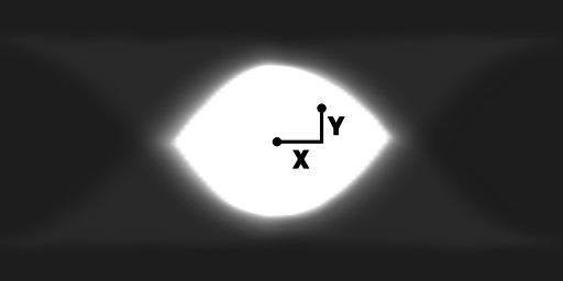
The figure above is an example of an eye pattern obtained using a Xilinx FPGA. You can see that the eye is open and the signal integrity is good. Since the signal quality is so good in this case, you could sample at slightly the wrong time, or the voltage threshold you use to distinguish a 1 from a 0 could be slightly off, and you would still receive the correct data.
All transceivers must have a sampler to determine of the received bit is a 1 or a 0. The eye scan circuitry provides another sampler with a fairly descriptive name - the “offset sampler”. This sampler can be offset relative to the ideal point at the middle of the eye. The horizontal offset (X) controls the timing lead or lag for when the sample is taken. The vertical offset (Y) controls the voltage threshold that the sample is compared with to decide whether it is a 1 or a 0. These offsets and the offset sampler value are accessible through the FPGA fabric.
An eye scan is performed while the transceiver is receiving data normally. We scan the horizontal and vertical offsets of the offset sampler, as shown in the diagram above, through their full range. The eye scan circuitry has a few modes. The one used for the scan above counts the number of times that the bit at the offset sampler differs from the ideal sample in the middle of the eye. If these differ, then there is an error and we draw a dark pixel at this X, Y position.
Waveforms
The eye described above is called a statistical eye. You are viewing a single bit period and it is effectively an average created by overlaying millions of bits. What we want is slightly more difficult - a waveform - multiple bits long and not the result of averaging.
At first glance it might seem that we cant do this with the eyescan circuitry, but there’s a trick. The Xilinx GTY docs contain a few references to “waveform view”, but in typical Xilinx fashion, they don’t really tell you anything useful that you could actually use to implement it. Incidentally, it was these remarks in the docs about waveforms that got me interested in this project in the first place.
So, in the next section I implement my guess for what they had in mind for extracting waveforms.
Waveform reception
Using another transceiver, we will transmit a repeating pattern and receive it with our eyescan transceiver. As with a statistical eye, the CDR circuitry will lock onto the bits and receive them, and we will vary the position of our offset sampler relative to the ideal sample. However, we configure the eye circuitry a little differently than for the statistical eye:
- We use a mode which, instead of constantly triggering the offset sampler, records a sample only if the last N bits matches a configurable trigger pattern, where N can be set using a mask. This allows us to only sample when a certain bit pattern history occurs, instead of taking an average over all possible bits
- Instead of an error bit that indicates that the offset sample differed from the true sample, we just get the raw sample. This allows us to see the actual sliced bit value, rather than whether it agrees with the true bit value or not.
As with the statistical eye, we sweep horizontally throughout a bit period to get the waveform at a certain X position. To sweep through multiple bits, we swizzle a mask in the eyescan logic which sets which bit in the 32 bit window we are looking at.
We only get a 1 or a 0 for each X offset we sample. A real sampling oscilloscope would give us an analog value - something continuous. To obtain an analog value, we also sweep the Y offset (which sets the comparator threshold) through it’s range. Conceptually, the Y value where the offset sampler is giving us a mixture of 0s and 1s is where the Y value approximately matches the waveform voltage.
So, a regular sampling oscilloscope sweeps through different time offsets (X) in a periodic signal. Ours does that too, but also sweeps through the Y range looking for the transition from 1 to 0 to emulate an analog sampler.
A raw plot of 1 counts for the trigger pattern 0xA2 looks like this:
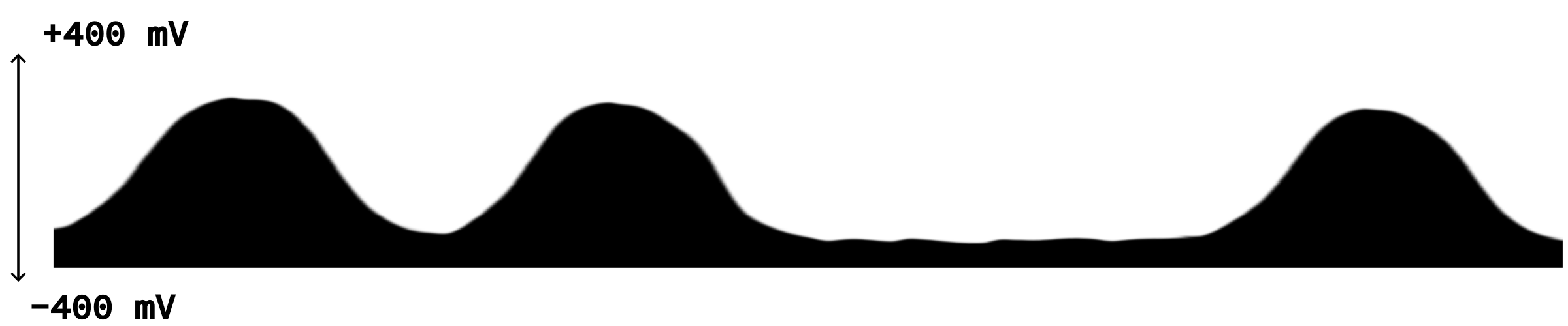
Dark areas are where the offset sampler returned mostly ones. Light areas are mostly zeros.
If we are sampling below the true waveform, we expect the slicer to always return a 1, so this part of the graph is dark. If we are above the true waveform, we expect 0s, so this will be white. Near the wave, we expect a transition from all 1s to all 0s, i.e. a black to white transition as in the figure above.
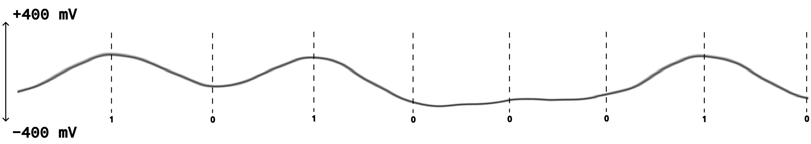
To get an actual wave, I have applied an image processing edge detection algorithm. Where the counts are changing rapidly from high to low is where the actual waveform is and therefore these X, Y offsets have large values after applying the edge detection algorithm. A waveform emerges!
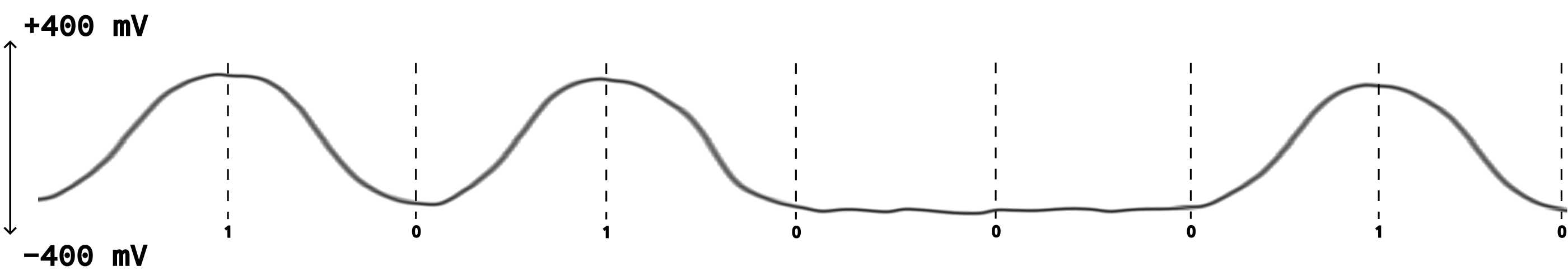
This is an analog wave that shows the time domain waveform as it is received at the transceiver.
Transmission
On the transmit side, where we generate the periodic waveforms we are sampling, we need to ensure our trigger pattern occurs regularly so we get enough samples to scan the entire range in a reasonable amount of time.
Additionally, to ensure we are always sampling the same periodic waveform (just at different offsets), we need to ensure that each time we trigger, the sequence of bits leading up to the trigger was the same, for at least the duration of the channel’s impulse response.
PRBS patterns achieve both of these requirements perfectly. Suppose you use PRBS-9, then any given 9 bit trigger pattern will repeat every 511 bits. So, you get regular repetitions of the trigger pattern. Also, since the 9 bit pattern occurs exactly once in the repeating 511 bit pattern, the bits proceeding the trigger pattern will be the same every time.
Experiments!
SFP loopback
The waveform above is generated using a 3m DAC (direct attach copper) cable at 10G. You can see that the waveform is fairly “curvy” as high frequencies are attenuated. Let’s also try a SFP loopback at the same data rate, which will provide the shortest possible path. Since the board has excellent signal integrity I’m expecting a very clean waveform.
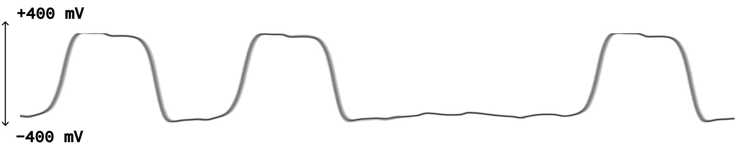
As you can see, it did not disappoint. It approximates a square wave for our bit pattern. After each bit transition, it quickly saturates to a 1 or a 0 and there is a massive timing margin around the optimal sampling point in the middle where the sampler would still return the correct data. Also, there is less attenuation over the shorter connection so the amplitude is greater than in the diagram for the 3m cable. It even gets clipped at points.
Higher data rates
Let’s double the data rate to 20G, while keeping the 3m cable. Note that we are still using a 10G DAC cable (I don’t have a 25G one). Unsurprisingly, the transceiver struggles and is unable to lock onto the bits. However, if we turn the linear equalizer on, the transceiver is able to receive the data correctly at 20G.
By default, Xilinx transceivers have equalization turned on, but in order to make sure the waveforms above accurately reflect the received voltages, I turned it off. Since the equalizer is back on for the higher rate waveform below, it doesn’t represent the exact voltages received at the transceiver’s pins. The equalizer will be altering the waveform a little in order to open the eye.
This time, you can see the waveform is even more curvy than the 10G one because high frequencies are being attenuated even more. Still, the bit pattern can be clearly distinguished and would be received without many (or any?) bit flips.
I’ve also included a statistical eye for this 20G 3m case below. You can see that the eye is nearly closed so we are approaching the limit of what the transceiver can handle without errors. Still, I’m pretty impressed that the transceiver can correctly receive data over three meters at twice the rate supported by the cable.

Conclusion
I’ve demonstrated that it’s possible to effectively build a high speed sampling oscilloscope using only the transceivers on a Xilinx FPGA. It’s a nice tool to quantify the effect of cables, data rates, and equalization. I also think it’s very nice to be able to see what these absurdly fast signals are doing in the time domain.
In the future, I’d like to have a go at designing a PCB with some high speed serial traces. This will be a valuable tool for characterising and debugging my links.